_1673427121.png)
Materials
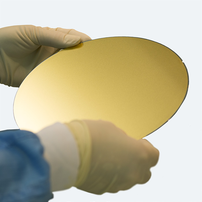
Our Silicon wafers
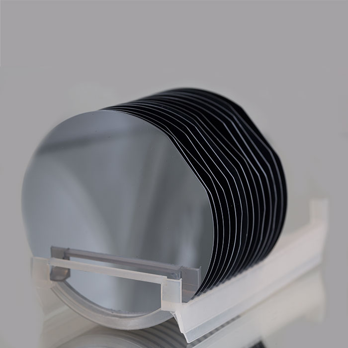
Description
-
Orientation : <100>
- Growth method : CZ and FZ
- Resistivity: from 0.001 to > 20 000 Ω.cm
- With flats
- Packaging : 25 pieces/box
We can offer wafers with some other parameters. Please fill in the table "Our customized products", with your specifications.
From single crystals to polished Wafers GrindingThe ingots grown with the Czochralski or float-zone technique are ground to the desired diameter and cut into shorter workable cylinders with e. g. a band saw and ground to a certain diameter. An orientation flat is added to indicate the crystal orientation (schema right), while wafers with an 8 inch diameter and above use a single notch to convey wafer orientation, independent from the doping type.
Dicing
Two common techniques are applied for wafer dicing: Inside hole saw and wire saw, both explained in the following sections.
Inside Hole Saw (Annular Saw) :The wafers are sawed inside a circular blade whose cutting edge is filled with diamond splinters (schema right). After sawing, the wafer surfaces are already relatively flat and smooth, so the subsequent lapping of the surfaces takes less time and effort. However, only one wafer per annular saw can be cut at the same time, so this technique has a comparably low throughput which makes the wafers more expensive compared to wafers cut by a wire saw.
Wire SawIn order to increase throughput, wire saws with many parallel wires are used which cut many wafers at once (schema right). A long (up to 100 km) high-grade steel wire with a diameter of » 100 - 200 μm is wrapped around rotating rollers with hundreds of equidistant grooves at a speed of typically 10 m/s. The mounted silicon cylinder is drained into the wire grid and thus cut into single wafers.
The wire is either coated with diamond splinters or wetted with a suspension of abrasive particles such as diamonds or silicon carbide grains, and a carrier (glycol or oil).
The main advantage of this sawing method is that hundreds of wafers can be cut at a time with one wire. However, the attained wafer surface is less smooth and more bumpy as compared to wafers cut by an annular saw, so the subsequent lapping takes more time.
Lapping
After dicing, the wafers are lapped on both sides in order to i) remove the surface silicon which has been cracked or otherwise damaged by the slicing process (e. g. grooves by the wire saw) and ii) thinned to the desired wafer thickness. Several wafers at a time are lapped in between two counter-rotating pads by a slurry consisting of e. g. Al2O3 or SiC abrasive grains with a defined size distribution.
EtchingWafer dicing and lapping degrade the silicon surface crystal structure, so subsequently the wafers are etched in either KOH- or HNO3/HF based etchants in order to remove the damaged surface.
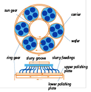
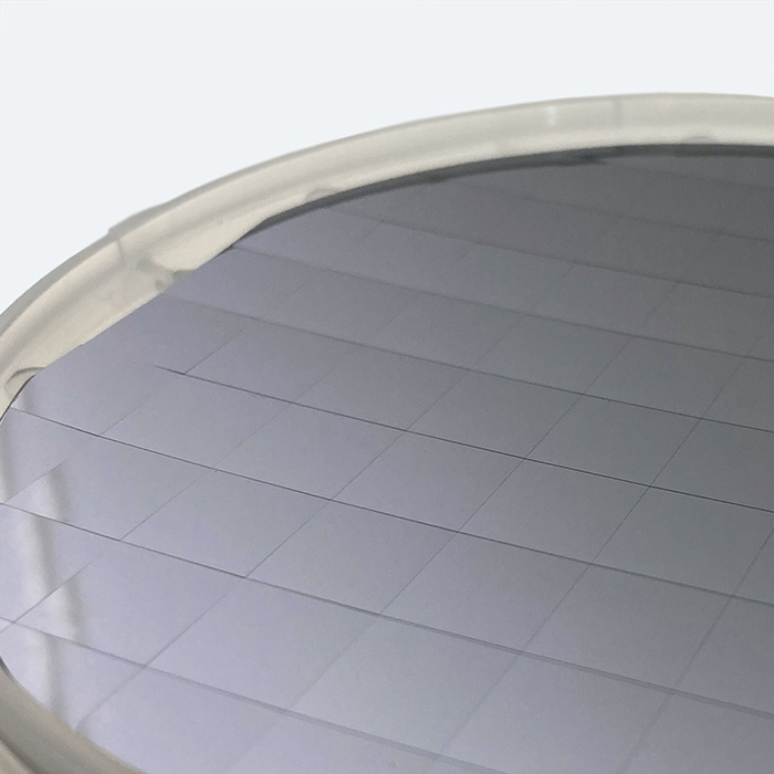
PolishingAfter etching, both wafer surfaces appear like the rear side of finished single-side polished wafer. In order to attain the super-flat, mirrored surface with a remaining roughness on atomic scale, the wafers have to be polished. Wafer polishing is a multi-step process using an ultra-fine slurry with 10 - 100 nm sized grains consisting of e. g. Al2O3, SiO2 or CeO2 which, combined with pressure, erode and mechanically and chemically smoothen the wafer surface between two rotating pads.
CleaningFinally, the wafers are cleaned with ultra-pure chemicals in order to remove the polishing agents thereby making them residual-free.
This product is available in 24 versions
See our references- Our standards
- Description
- Linked products
Our standards
| P/N | Ø | Thick. (µm) | Type / Dopant | polish. sides | Res. (Ω.cm) | Ra (nm) | Quantity | |
|---|---|---|---|---|---|---|---|---|
|
P/N WAFERS2-2FPIn stock |
Ø2" | Thick. (µm)280 | Type / Dopantn-P | polish. sides2 | Res. (Ω.cm)1-20 | Ra (nm)< 0.5 | Quantity | Add to cart |
|
P/N WAK2PNIn stock |
Ø2" | Thick. (µm)280 | Type / Dopantn-P | polish. sides1 | Res. (Ω.cm)1-20 | Ra (nm)< 4 | Quantity | Add to cart |
|
P/N WAK2PPIn stock |
Ø2" | Thick. (µm)280 | Type / Dopantp-B | polish. sides1 | Res. (Ω.cm)1-20 | Ra (nm)< 4 | Quantity | Add to cart |
|
P/N WAK2NFRIn stock |
Ø2" | Thick. (µm)300 | Type / Dopantn-As | polish. sides1 | Res. (Ω.cm)0.001-0.005 | Ra (nm)< 4 | Quantity | Add to cart |
|
P/N WAK2PFRIn stock |
Ø2" | Thick. (µm)275 | Type / Dopantp-B | polish. sides1 | Res. (Ω.cm)0.03-0.05 | Ra (nm)< 4 | Quantity | Add to cart |
|
P/N WAS2In stock |
Ø2" | Thick. (µm)280 | Type / Dopantn-P | polish. sides1 | Res. (Ω.cm)1-10 | Ra (nm)< 1 | Quantity | Add to cart |
| P/NWAFERS2-NFR | Ø2" | Thick. (µm)300 | Type / Dopantn-As | polish. sides1 | Res. (Ω.cm)0.001-0.005 | Ra (nm)< 0.5 | Quantity | Add to cart |
|
P/N WAS2PIRIn stock |
Ø2" (FZ) | Thick. (µm)280 | Type / Dopantn-P | polish. sides2 | Res. (Ω.cm)> 100 | Ra (nm)< 0.5 | Quantity | Add to cart |
|
P/N WAK2PHRIn stock |
Ø2" (FZ) | Thick. (µm)300 | Type / Dopantp-B | polish. sides1 | Res. (Ω.cm)4000 | Ra (nm)<4 | Quantity | Add to cart |
| P/NWAK2PN2FP | Ø2" | Thick. (µm)280 | Type / Dopantn-P | polish. sides2 | Res. (Ω.cm)1-20 | Ra (nm)<4 | Quantity | Add to cart |
|
P/N WAK2PP-2FPIn stock |
Ø2" | Thick. (µm)280 | Type / Dopantp-B | polish. sides2 | Res. (Ω.cm)1-20 | Ra (nm)< 4 | Quantity | Add to cart |
|
P/N WAP2FZIn stock |
Ø2" (FZ) | Thick. (µm)280 | Type / Dopantintrinsic | polish. sides1 | Res. (Ω.cm)> 20 000 | Ra (nm)< 0.5 | Quantity | Add to cart |
|
P/N WAP2FZ-2FPIn stock |
Ø2" (FZ) | Thick. (µm)280 | Type / Dopantintrinsic | polish. sides2 | Res. (Ω.cm)> 20 000 | Ra (nm)< 0.5 | Quantity | Add to cart |
|
P/N WAK3PNIn stock |
Ø3" | Thick. (µm)380 | Type / Dopantn-P | polish. sides1 | Res. (Ω.cm)1-20 | Ra (nm)< 4 | Quantity | Add to cart |
|
P/N WAK3PN-2FPIn stock |
Ø3" | Thick. (µm)1000 | Type / Dopantn-P | polish. sides2 | Res. (Ω.cm)Indifferent | Ra (nm)< 4 | Quantity | Add to cart |
|
P/N WAK3PPIn stock |
Ø3" | Thick. (µm)380 | Type / Dopantp-B | polish. sides1 | Res. (Ω.cm)5-10 | Ra (nm)<4 | Quantity | Add to cart |
|
P/N WAS3N40+In stock |
Ø3" | Thick. (µm)380 | Type / Dopantp-B | polish. sides1 | Res. (Ω.cm)Indifferent | Ra (nm)< 1 | Quantity | Add to cart |
|
P/N WAK4PNIn stock |
Ø4" | Thick. (µm)525 | Type / Dopantn-P | polish. sides1 | Res. (Ω.cm)1-20 | Ra (nm)< 4 | Quantity | Add to cart |
|
P/N WAK4PPIn stock |
Ø4" | Thick. (µm)525 | Type / Dopantp-B | polish. sides1 | Res. (Ω.cm)1-20 | Ra (nm)< 4 | Quantity | Add to cart |
|
P/N WAK4NFRIn stock |
Ø4" | Thick. (µm)500 | Type / Dopantn-As | polish. sides1 | Res. (Ω.cm)<0.005 | Ra (nm)< 4 | Quantity | Add to cart |
|
P/N WAK4PFRIn stock |
Ø4" | Thick. (µm)525 | Type / Dopantp-B | polish. sides1 | Res. (Ω.cm)< 0.005 | Ra (nm)< 4 | Quantity | Add to cart |
| P/NWAS4P1020 | Ø4" | Thick. (µm)525 | Type / Dopantn-P | polish. sides1 | Res. (Ω.cm)10-20 | Ra (nm)< 0.5 | Quantity | Add to cart |
|
P/N WAP4FZIn stock |
Ø4" (FZ) | Thick. (µm)525 | Type / Dopantintrinsic | polish. sides1 | Res. (Ω.cm)> 20 000 | Ra (nm)< 0.5 | Quantity | Add to cart |
| P/NWAP4FZ-2FP | Ø4" (FZ) | Thick. (µm)525 | Type / Dopantintrinsic | polish. sides2 | Res. (Ω.cm)> 20 000 | Ra (nm)< 0.5 | Quantity | Add to cart |
Create your custom product
| Diameter & Thickness
ex: 2'', 100 µm |
Polished sides, flatness
ex: 2 PS, 2 SEMI |
Other specifications
Enter orientation, growth method, resistivity, type, dopant, ... |
Quantity | |
|---|---|---|---|---|
| Diameter & Thickness | Polished sides, flatness | Other specifications | Quantity | Add to cart |
Can't find the desired product? Contact us
Description
Main specifications for our wafers in stock:
-
Orientation : <100>
- Growth method : CZ and FZ
- Resistivity: from 0.001 to > 20 000 Ω.cm
- With flats
- Packaging : 25 pieces/box
We can offer wafers with some other parameters. Please fill in the table "Our customized products", with your specifications.
From single crystals to polished Wafers
Grinding
The ingots grown with the Czochralski or float-zone technique are ground to the desired diameter and cut into shorter workable cylinders with e. g. a band saw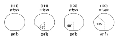 and ground to a certain diameter. An orientation flat is added to indicate the crystal orientation (schema right), while wafers with an 8 inch diameter and above use a single notch to convey wafer orientation, independent from the doping type.
Dicing
Two common techniques are applied for wafer dicing: Inside hole saw and wire saw, both explained in the following sections.
Inside Hole Saw (Annular Saw) : 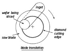
The wafers are sawed inside a circular blade whose cutting edge is filled with diamond splinters (schema right). After sawing, the wafer surfaces are already relatively flat and smooth, so the subsequent lapping of the surfaces takes less time and effort. However, only one wafer per annular saw can be cut at the same time, so this technique has a comparably low throughput which makes the wafers more expensive compared to wafers cut by a wire saw.
Wire Saw
In order to increase throughput, wire saws with many parallel wires are used which cut many wafers at once (schema right). A long (up to 100 km) high-grade steel wire with a diameter of » 100 - 200 μm is wrapped around rotating rollers with hundreds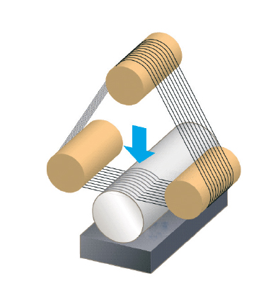 of equidistant grooves at a speed of typically 10 m/s. The mounted silicon cylinder is drained into the wire grid and thus cut into single wafers.
The wire is either coated with diamond splinters or wetted with a suspension of abrasive particles such as diamonds or silicon carbide grains, and a carrier (glycol or oil).
The main advantage of this sawing method is that hundreds of wafers can be cut at a time with one wire. However, the attained wafer surface is less smooth and more bumpy as compared to wafers cut by an annular saw, so the subsequent lapping takes more time.
Lapping
After dicing, the wafers are lapped on both sides in order to i) remove the surface silicon which has been cracked or otherwise damaged by the slicing process (e. g. grooves by the wire saw) and ii) thinned to the desired wafer thickness. Several wafers at a time are lapped in between two counter-rotating pads by a slurry consisting of e. g. Al2O3 or SiC abrasive grains with a defined size distribution.
Etching
Wafer dicing and lapping degrade the silicon surface crystal structure, so subsequently the wafers are etched in either KOH- or HNO3/HF based etchants in order to remove the damaged surface.
Polishing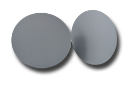
After etching, both wafer surfaces appear like the rear side of finished single-side polished wafer. In order to attain the super-flat, mirrored surface with a remaining roughness on atomic scale, the wafers have to be polished. Wafer polishing is a multi-step process using an ultra-fine slurry with 10 - 100 nm sized grains consisting of e. g. Al2O3, SiO2 or CeO2 which, combined with pressure, erode and mechanically and chemically smoothen the wafer surface between two rotating pads.
Cleaning
Finally, the wafers are cleaned with ultra-pure chemicals in order to remove the polishing agents thereby making them residual-free.
Linked products
Thermal oxidation
Silicon nitride Si3N4 layers
Vacuum coatings on wafers and silicon substrates
Dicing of wafers and silicon substrates
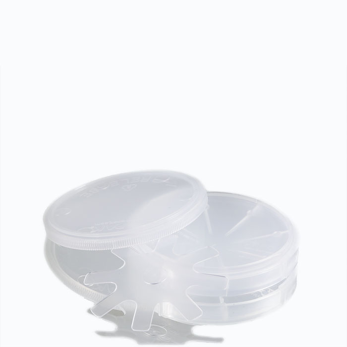
Single Silicon wafer and susbstrate container
If you want an offer, or more information on this product, contact us:
Fast delivery
in France and Europe
ISO 9001
and 14001 certifications
Service / Maintenance of
mechanical components