_1673427121.png)
Materials
Thermal oxidation
Description
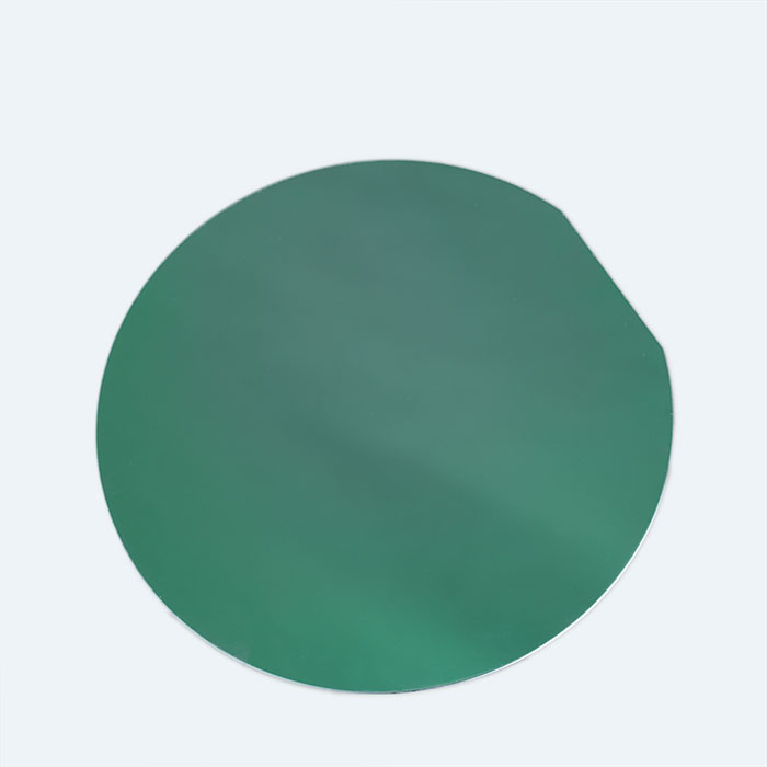
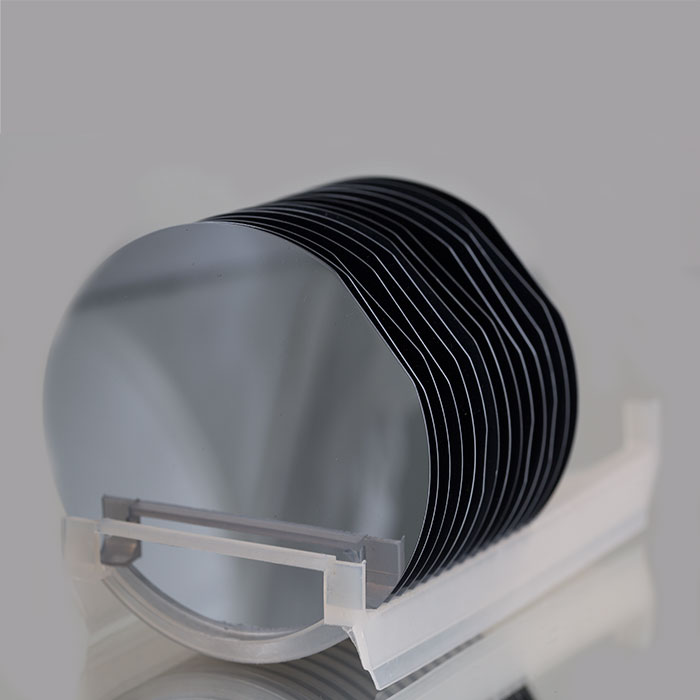
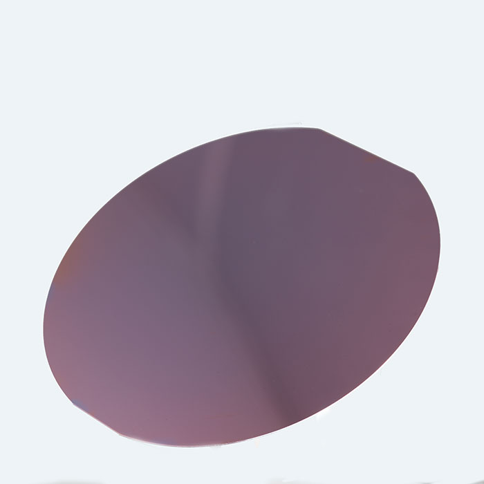
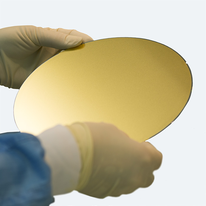
We offer a service of thermal oxidation (by dry or wet way) on our wafers (or on your wafers). The oxidation thickness can be from 50 nm to 5 µm. The oxidation on one side is also possible.
Thermal Oxidation of Silicon : Fields of ApplicationThe electronic (resistivity 1014 ... 1016 Ohm.cm, breakthrough field 106 ... 107 V/cm, barrier for electrons and holes from crystalline Si > 3 eV), mechanical (melting point approx. 1700°C) and optical (transparent in the visible as well as near infrared and ultraviolet spectral range) properties of SiO2 make it a suitable material for the dielectric film in transistors, capacitors (DRAM) or flash-memories; and as a hard mask for diffusion, implantation, wet or dry chemical etching; and generally as an isolator between integrated devices, or as an antireflection layer on e. g. solar cells.
Required SiO2 film thicknesses range from a few nm (gate-oxide of state-of-the-art CMOS transistors) up to several μm for electrical insulation. Compared to sputtered or CVD SiO2, thermal SiO2 reveals a better and more reproducible electrical insulation.
Oxidation Technique
Compared to (crystalline) quartz, native (= few nm grown at room temperature in air) and thermal (growth temperature 800 - 1200°C) silicon dioxide (schema of an oxidation furnace right) is amorphous (= without longterm atomic lattice order). The silicon in native or thermally grown SiO2 evolves from the Si substrate, which is partially consumed during SiO2 growth: 100 nm SiO2 requires approx. 46 nm Si, while the wafer thickness simultaneously increases by approx. 54 nm. One has to distinguish between dry oxide (Si + O2 à SiO2), and – with H2O as process gas – wet oxide (Si + 2 H2O à SiO2 + 2 H2). At the same process parameters, due to the higher growth rate, wet oxide reveals a higher porosity and HF etch rate.
- Our standards
- Description
- Linked products
- Linked categories
Create your custom product
| Diameter wafer
|
Oxidation thickness
|
Number of oxidised faces
|
Quantity | |
|---|---|---|---|---|
| Diameter wafer | Oxidation thickness | Number of oxidised faces | Quantity | Add to cart |
Can't find the desired product? Contact us
Description
We offer a service of thermal oxidation (by dry or wet way) on our wafers (or on your wafers). The oxidation thickness can be from 50 nm to 5 µm. The oxidation on one side is also possible.
Thermal Oxidation of Silicon :
Fields of Application
The electronic (resistivity 1014 ... 1016 Ohm.cm, breakthrough field 106 ... 107 V/cm, barrier for electrons and holes from crystalline Si > 3 eV), mechanical (melting point approx. 1700°C) and optical (transparent in the visible as well as near infrared and ultraviolet spectral range) properties of SiO2 make it a suitable material for the dielectric film in transistors, capacitors (DRAM) or flash-memories; and as a hard mask for diffusion, implantation, wet or dry chemical etching; and generally as an isolator between integrated devices, or as an antireflection layer on e. g. solar cells.
Required SiO2 film thicknesses range from a few nm (gate-oxide of state-of-the-art CMOS transistors) up to several μm for electrical insulation. Compared to sputtered or CVD SiO2, thermal SiO2 reveals a better and more reproducible electrical insulation.
Oxidation Technique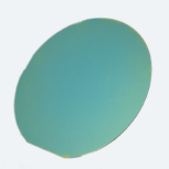
Compared to (crystalline) quartz, native (= few nm grown at room temperature in air) and thermal (growth temperature 800 - 1200°C) silicon dioxide (schema of an oxidation furnace right) is amorphous (= without longterm atomic lattice order). The silicon in native or thermally grown SiO2 evolves from the Si substrate, which is partially consumed during SiO2 growth: 100 nm SiO2 requires approx. 46 nm Si, while the wafer thickness simultaneously increases by approx. 54 nm. One has to distinguish between dry oxide (Si + O2 à SiO2), and – with H2O as process gas – wet oxide (Si + 2 H2O à SiO2 + 2 H2). At the same process parameters, due to the higher growth rate, wet oxide reveals a higher porosity and HF etch rate.
Linked products
Our Silicon wafers
Silicon nitride Si3N4 layers
Vacuum coatings on wafers and silicon substrates
Dicing of wafers and silicon substrates
Linked categories
Wafers tweezers
If you want an offer, or more information on this product, contact us:
Fast delivery
in France and Europe
ISO 9001
and 14001 certifications
Service / Maintenance of
mechanical components